Physical Vapor Deposition (PVD): Explore the Process, Benefits and Applications
Have you ever wondered how particular objects get their shiny and durable surfaces? The answer lies in a fascinating process called Physical Vapor Deposition (PVD). This article will take you on a journey to explore the functions and applications of PVD in various industries. We'll dive deep into the PVD process, its underlying principles, and the techniques involved. By the end, you'll have a comprehensive understanding of how PVD works and why it is crucial to comprehend its functions and applications.
Understanding the PVD Process
PVD, also known as Physical Vapor Deposition, is a deposition technique that involves the vaporization of a solid material and its subsequent condensation on a substrate. The process relies on the principles of physical evaporation and condensation to create thin films with unique properties. Let's break down the PVD process step-by-step to understand it better.
Firstly, a vacuum chamber creates a controlled environment devoid of air and impurities. This chamber plays a crucial role in maintaining the integrity of the PVD process. The next step involves heating the source material, known as the target or the evaporative source, to a high temperature. As the target heats up, its atoms or molecules gain sufficient energy to break free from the surface and enter the vapor phase.
Once in the vapor phase, the atoms or molecules travel through the vacuum chamber and eventually reach the substrate. Typically, the substrate is a solid material positioned in the chamber to receive the vaporized material. Upon reaching the substrate, the vaporized particles condense, forming a thin film layer. The film grows atom-by-atom, gradually covering the substrate's surface with the desired material.
Different PVD techniques and their variations exist, each with its own unique set of characteristics. Some standard PVD techniques include sputtering, evaporation, and ion plating. Sputtering involves bombarding the target material with high-energy ions to release its atoms or molecules. On the other hand, evaporation relies on heating the target material until it reaches its vaporization point. Ion plating combines the principles of sputtering and evaporation, creating a more controlled deposition process.
Classification of the PVD Process
Sputtering coating
Sputtering coating refers to the process of using kinetic energy particles (such as argon ions) to bombard the surface of the target material under vacuum conditions so that the atoms on the surface of the target material can obtain enough energy to escape, which is called sputtering. Argon (Ar) is filled under vacuum conditions, and the argon is glow-discharged under high voltage, which can ionize the argon (Ar) atoms into argon ions (Ar+). Under the action of the electric field force, the argon ions accelerate the bombardment of the cathode target made of plating material, and the target material will be sputtered out and deposited on the surface of the workpiece.
The sputtered target is deposited on the substrate's surface, called sputter coating. The incident ions in the sputtering coating are generally obtained by glow discharge in the range of 10-2Pa ~ 10Pa. Hence, the sputtered particles quickly collide with the gas molecules in the vacuum chamber while flying to the substrate, resulting in the random movement direction so that the deposited film is easily uniform. The developed large-scale magnetron sputtering coating has a high deposition rate, good process repeatability, and is easy to automate. It has been applied to large-scale architectural decoration and functional coating of industrial materials, such as TGN-JR type with multi-arc or magnetron. The production and preparation of nickel-plated Ni and silver Ag on the surface of foamed plastics and fiber fabrics of coils by sputtering.
The sputtering coating can be divided into DC, radio frequency, and magnetron sputtering. The corresponding glow discharge voltage source and control field are high voltage direct current, radio frequency (RF) alternating current, and magnetron control field.
Plasma coating
Cold cathode arc evaporation is usually used in physical vapor deposition, and the solid plating material is used as the cathode to form many bright spots on the surface of the cold cathode, that is, cathode arc spots. The arc spot is the arc root of the arc near the cathode. Under vacuum conditions, the arc is struck by an arced needle to make an arc discharge between the vacuum gold wall (anode) and the plating material (cathode), and multiple cathode arc spots rush on the surface of The cathode continuously and rapidly evaporating the plating material, making it Ionized into an arc plasma with plating material as the main component, and can quickly deposit the plating material on the substrate.
The current density in a tiny space is exceptionally high; the arc spot size is tiny, estimated to be about 1 μm to 100 μm, and the current density is as high as 105A/cm2 to 107A/cm2. Each arc spot exists. For a very short time, it explosively evaporates the plating material at the correction point of the ionized cathode, evaporates the ionized metal ions, and generates new arc spots on the surface of the cathode. Many arc spots continue to appear and disappear. So it is also called multi-arc evaporation. The earliest-designed plasma accelerator-type multi-arc evaporation ionization source is equipped with a magnetic field behind the cathode so that the evaporated ions can obtain the Hall acceleration effect, which is beneficial for the ion to increase as the energy to bombard the volume. Ionization source coating has a high ionization rate, called arc plasma coating. Because plasma coating often produces multi-arc spots, it is also called multi-arc evaporation ionization process.
Ion plating
The basic principle of ion plating is to use some plasma ionization technology under vacuum conditions to ionize the atoms of the plating material into ions partially and, at the same time, generate many high-energy neutral atoms and apply a negative bias voltage on the substrate to be plated. In this way, under the action of deep negative bias, ions are deposited on the surface of the substrate to form a thin film.
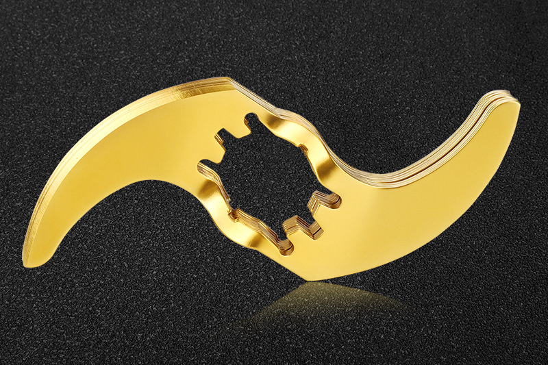
With the help of inert gas glow discharge, the ion coating vaporizes, evaporates, and ionizes the plating material (such as metal titanium). An electric field accelerates the ions and bombards the surface of the workpiece with high energy. At this time, if reactive gases such as carbon dioxide and nitrogen are introduced, the TiC and TiN coatings can be obtained on the surface of the workpiece with a hardness of up to 2000HV. Such as meat grinder blade PVD processing application.
Ion coating is the most widely used coating process in metal injection molding parts PVD processing.
Features
The primary feature of ion coating is to use some methods (such as electron beam evaporation, magnetron sputtering, multi-arc evaporation ionization, etc.) to ionize neutral particles into ions and electrons. A negative bias must be applied to the substrate to make the ions. The substrate is bombarded. The negative bias voltage is appropriately lowered so that the ions are deposited on the substrate to form a film, which is suitable for the surface treatment process of high-speed steel tools, hot forging dies, and other materials.
The advantages of ion plating are as follows:
The bond between the film layer and the substrate is strong, and the reaction temperature is low.
The film layer is uniform and dense.
The coiling property is suitable under the action of negative bias.
No pollution.
A variety of substrate materials are suitable for ion plating.
Functions of PVD
PVD serves various functions across different industries thanks to its ability to enhance surfaces, deposit thin films, and add decorative finishes. Let's explore the critical functions of PVD in detail.
Surface enhancement and modification
PVD is widely used to enhance the properties of surfaces, making them harder, more wear-resistant, and more durable. By depositing thin films of materials like titanium nitride (TiN), chromium nitride (CrN), or diamond-like carbon (DLC), PVD significantly improves the hardness and wear resistance of surfaces. This makes PVD-treated components ideal for applications in industries such as aerospace, cutting tools, and medical implants.
Moreover, PVD coatings offer enhanced corrosion resistance, protecting surfaces from degradation caused by moisture, chemicals, or environmental factors. Components subjected to harsh conditions, such as marine equipment, automotive parts, and oil and gas pipelines, greatly benefit from PVD's corrosion-resistant properties.
Thin film deposition
PVD excels in depositing thin films of various materials onto substrates. These thin films serve multiple purposes, such as providing functional coatings for optical, electrical, or mechanical applications. For example, due to their excellent electrical conductivity and optical transparency, PVD-deposited films of indium tin oxide (ITO) are commonly used in electronic displays, solar cells, and touchscreens.
In addition, PVD can create barrier layers to prevent moisture and gas permeation. These barriers find applications in the packaging industry, where PVD-coated films are used as protective layers for food, pharmaceuticals, and other sensitive products. By effectively sealing the package, PVD coatings ensure product freshness and longevity.
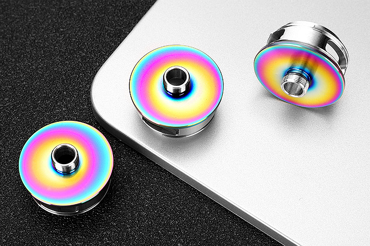
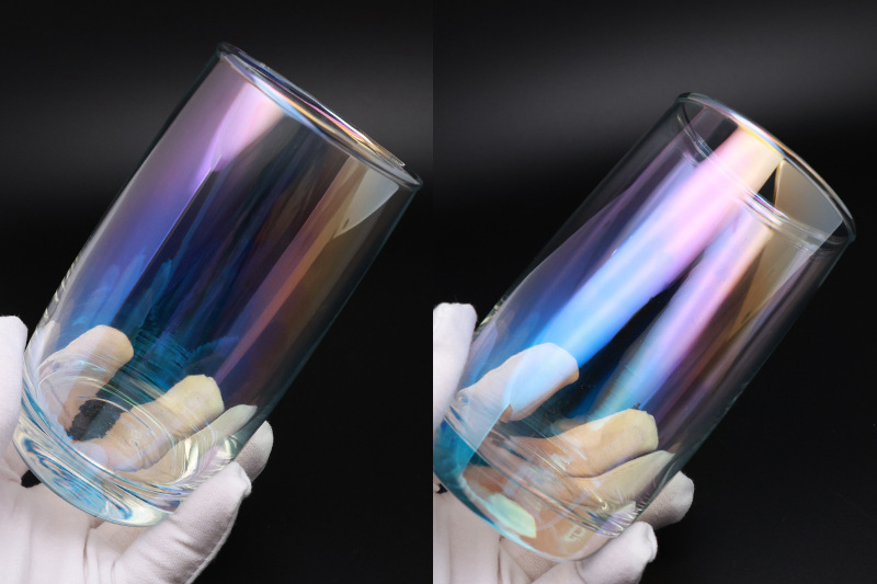
Decorative and aesthetic applications
PVD opens up a world of possibilities for decorative and aesthetic enhancements. The ability to deposit thin films of metals like gold, silver, or titanium onto various surfaces allows for customization and personalization. Jewelry watches and consumer electronics benefit from PVD coatings, which provide a luxurious and scratch-resistant finish.
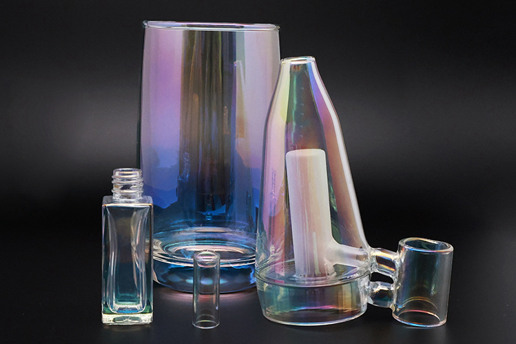
Moreover, industries such as automotive and architecture utilize PVD to create customized finishes on metal surfaces. With PVD, car manufacturers can offer unique paint alternatives, and architects can transform building facades into visually stunning structures. The versatility of PVD in achieving various colors, textures, and patterns makes it a favored choice for aesthetic applications.
Difference Between PVD and CVD
While PVD and CVD (Chemical Vapor Deposition) are both deposition techniques, they fundamentally differ. Let's compare PVD and CVD in terms of their principles and characteristics:
PVD | CVD |
|---|---|
Physical vaporization | Chemical reaction |
Deposition from vapor phase | Deposition from reactant gases |
Low temperature operation | High temperature operation |
Coating thickness control | Coating thickness uniformity |
Wide material compatibility | Greater material versatility |
Difference Between PVD Plating and Electroplating
PVD plating and electroplating are two distinct methods of depositing thin films onto substrates. Here's a comparison between the two techniques:
PVD Plating | Electroplating |
|---|---|
Physical vapor deposition | Electrochemical deposition |
Vaporized target material | Dissolved metal ions |
Wide material compatibility | Limited to conductive metals |
High durability | Moderate durability |
Environmentally friendly | Chemical waste production |
Plastic injection molded parts and ceramic injection molded ceramic parts can be treated with PVD and are not suitable for electroless plating.
Advantages of PVD Processing
PVD processing offers several advantages that contribute to its widespread adoption across industries. Some key advantages include:
Customizable properties: PVD allows precise control over the deposited film's composition, thickness, and structure, enabling tailored properties for specific applications.
Low-temperature operation: PVD can be performed at relatively low temperatures, making it compatible with temperature-sensitive substrates.
Environmentally friendly: PVD is a clean and environmentally friendly process since it does not involve using harmful chemicals or producing toxic waste.
High adhesion and durability: PVD coatings exhibit excellent adhesion to substrates, ensuring long-lasting performance even under challenging conditions.
Limitations of PVD Processing
While PVD processing offers numerous benefits, it also has some limitations to consider:
Limited to certain materials: PVD is more suitable for metals and some ceramics, limiting its applicability to non-metallic materials.
Deposition rate constraints: PVD is a slow deposition process compared to other methods, which may be a limitation for high-volume production.
Equipment complexity and cost: Setting up and maintaining PVD equipment can be costly due to the sophisticated vacuum chambers and specialized components required.
Potential Applications in Emerging Industries
As emerging technologies advance, PVD finds potential applications in industries such as flexible electronics and nanotechnology. The ability to deposit thin films on flexible substrates makes PVD a valuable technique for manufacturing bendable displays, wearable devices, and flexible sensors.
In nanotechnology, PVD enables the precise deposition of thin films and nanostructures, making it a critical tool for fabricating nanoscale devices, sensors, and integrated circuits.